Green Nano TechnologyNano HydrogelsTrimeric PeptidesPetone MoleculesNano AyurvedaNano Functional FoodGreen Nano TechnologyNano HydrogelsTrimeric PeptidesPetone MoleculesNano Ayurveda
Twenty-five years of advanced scientific research have resulted in a patented, industry-ready Green Nanotechnology platform, enabling reproducible, scalable, and regulatory-aligned nano-manufacturing through eco-friendly synthesis routes.
The platform delivers application-ready nanomaterials and formulations with enhanced stability, controlled size, and improved bioavailability, serving healthcare, agriculture, hygiene, nutrition, and advanced materials markets.
Kadamba’s Green Nano platform supports technology licensing, co-development, and industrial scale-up, providing industries with low-carbon, IP-protected, and compliant nanomaterial solutions for sustainable and high-performance applications.

At Kadamba, we are at the forefront in pioneering sustainable advancements through the power of nanotechnology.


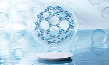
The power of advanced nanotechnology and natural ingredients creating hydrogels with unparalleled performance.
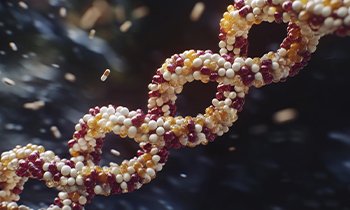
Transformative tools for nanoscale biomolecular engineering in next-gen therapeutics and diagnostics.

Kadamba has pioneered an exceptionally innovative process to produce a next generation energy product named “Petone”.

 NANO AYURVEDA
 Advanced nano therapeutics and wellness intelligence, delivering transformative, evidence-based healing. A Global-First Centre for Next-Generation Green Medicine NanoCare Clinic in Bangalore is Kadamba’s flagship, model wellness and integrative care centre, created to translate decades of patented green medicine research into real-world healing.

Converging Evidence
Based Inputs
Integration Workflow &
Signal Fusion
Holistic
Framework
Personalized Wellness
Mapping

Kadamba’s Integrated Bio-Rhythm Concept is a whole-person wellness mapping framework designed to read how the body’s regulation, energy stability, neuro-emotional state, and lived patterns evolve over time. Instead of relying on a single test or one clinical lens, Kadamba converges multiple evidence streams to construct a multi-layer bio-rhythm profile for each individual.
The core principle is simple: wellness is dynamic, so a reliable wellness profile must reflect interactions across physiology, mind-emotion, and systemic timing-not isolated symptoms.
This is a high-resolution wellness-profiling and decision-support system, built on converging parameters and validated internal interpretation frameworks.
Kadamba’s translational model fosters a dynamic synergy between academia
and industry, turning validated research into practical, scalable technologies.
By applying green nanoscience, this collaboration drives a new paradigm of
nature-aligned innovation—creating sustainable solutions, revolutionary
products, and next-generation businesses that deliver measurable impact
across healthcare, nutrition, agriculture, and environmental sectors.

Verified standards for safety, quality and trust.


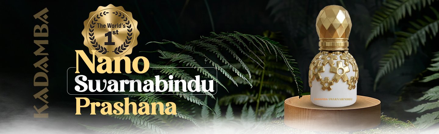

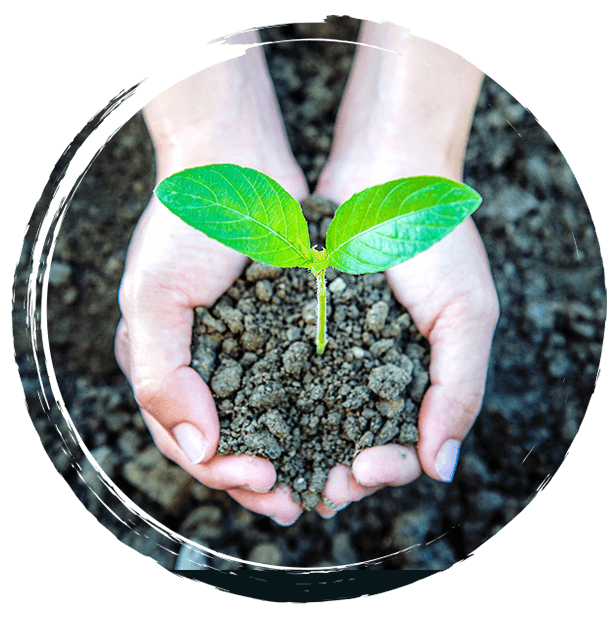
Kadamba transforms nature’s wisdom into green nanotechnology products-chemical-free, scientifically advanced and planet-friendly. Shop for our exclusive, internationally patented innovations directly online.